

WFE Equipment - Why This Time Is Different

The semiconductor equipment industry has trained investors to expect cyclicality. Memory builds, memory corrects. Logic expands, logic digests. The pattern has repeated with such regularity over the past three decades that it became axiomatic: what goes up must come down, and the prudent investor positions for reversion to the mean.
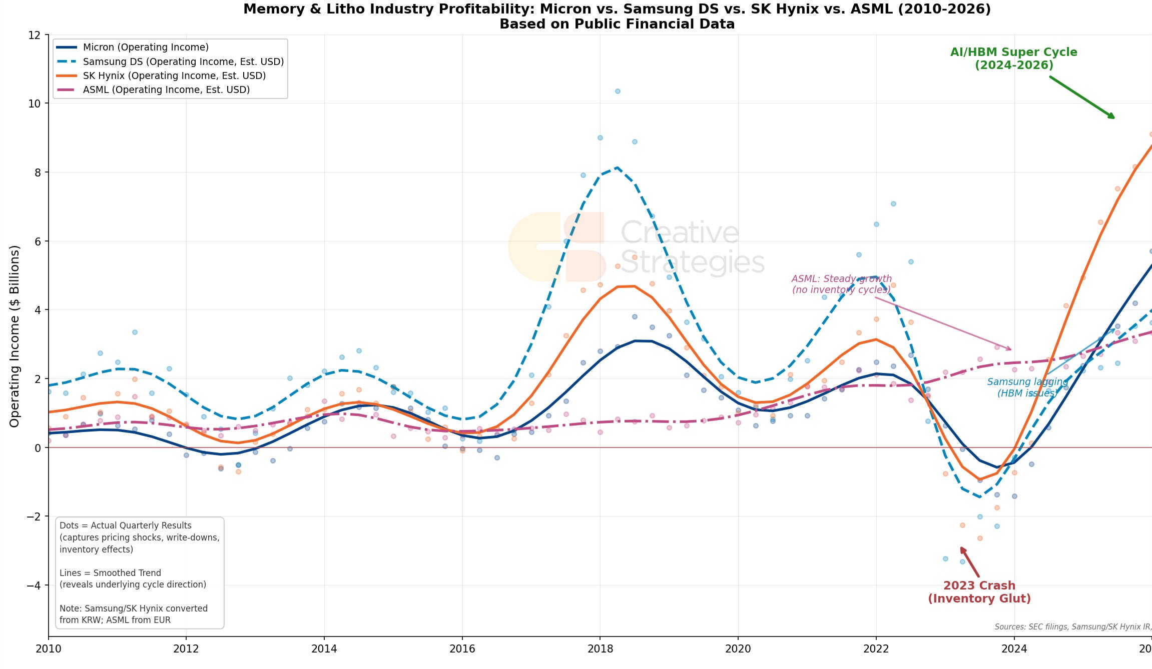
What happens to the right of this chart is one of the major discussions we regularly have with the industry and with investors.
What if this time is different? At least for much longer than many anticipate.
The wafer fab equipment market is entering a multi-year expansion phase that appears to represent a structural break from historical patterns. The strength of this position is the logical conclusion of three compounding dynamics that have fundamentally altered the economics of semiconductor manufacturing. The binding constraints on AI accelerator supply have created equipment demand that is now decoupled from wafer volume, and the implications for the WFE sector are significant.
The narrative from WFE players has always been leading toward the step changes in process technology coming, the Angstrom era, and how that will change the shape of demand for new tools. Things like the transition to Gate-All-Around transistors and Backside Power Delivery at the 2nm node are collapsing tool reuse rates in ways the industry has never experienced. Previous node transitions—N7 to N5, N5 to N3—maintained 50-70% tool overlap because they were evolutionary refinements of the same FinFET architecture. The move to N2 is different. It requires new epitaxial growth sequences, new selective etch chemistries, and new deposition configurations that render much of the existing installed base obsolete for critical layers. Capital intensity per 50,000 wafer capacity is rising from $16 billion at N5 to nearly $30 billion at N2. In many ways, the Angstrom era creates the need for a full, fresh semicap buildout.
Those in the weeds in the memory market recognize a similar story, though through a different mechanism. High Bandwidth Memory has become the single most critical bottleneck in the AI hardware stack, and the production economics compound the challenges. HBM3e consumes approximately three times the wafer capacity of standard DDR5 to produce an equivalent amount of bits. HBM4, which enters volume production this year, worsens that ratio to 4:1. The major memory manufacturers spent 2022-2024 in an extraordinarily conservative posture on greenfield expansion—balance sheet concerns, demand uncertainty, and inventory overhangs all contributed to restraint. That conservatism is now reversing as the AI demand signal has proven durable and HBM allocations have consumed existing capacity. DRAM bit growth is accelerating to levels not seen since the smartphone buildout era, and the equipment intensity per bit is rising simultaneously. This dynamic compounds in ways that favor sustained equipment demand.
Then there is NAND, which the market has largely written off as a secular loser to cloud storage and streaming. We see something different emerging. Enterprise SSDs for AI infrastructure are driving a demand recovery that will return NAND WFE to 2019-2021 levels by 2027. AI training clusters require massive local storage for dataset staging and checkpoint saving. Inference deployments demand high-performance flash for model loading and context caching. The storage intensity per AI server runs 3-5x that of traditional enterprise configurations. Enterprise demand is driving this cycle, layered on top of a recovering base.
As noted in our TSMC note, the packaging bottleneck adds another dimension entirely. Advanced packaging has eclipsed front-end lithography as the primary constraint on AI accelerator supply. TSMC is expanding CoWoS capacity aggressively—targeting 60%+ growth in 2026—yet the supply-demand gap may actually widen as next-generation architectures require larger interposer areas. The transition from CoWoS-S to CoWoS-L, driven by the physical limitations of lithography reticle sizes, is forcing architectural changes that reduce wafer-level yields and extend the capacity constraint deeper into the decade.
Because we seek to understand the depth of every constraint facing this industry, we have gone through the effort of quantifying these dynamics and their implications for the equipment vendors positioned to benefit. The analysis leads us to believe the market will move meaningfully above consensus forecasts for 2026 and 2027, with upside scenarios that would represent the largest market expansion in WFE history. The companies with exposure to the binding constraints—HBM production, DRAM greenfield, advanced packaging, and leading-edge logic—are positioned to capture a disproportionate share of this structural shift. The Angstrom era changes everything, and understanding why is essential to grasping why this time is different across the semiconductor industry.
The full report provides our complete framework.
What Subscribers Get in the Full Report:
Our base and bull case WFE market forecasts through 2028, with segment-level detail on DRAM, NAND, and Foundry Logic
Quantified analysis of the DRAM greenfield inflection and why bit growth is structurally accelerating
NAND recovery timing and the enterprise SSD demand thesis
CoWoS capacity trajectory with supply-demand gap projections through 2027
Capital intensity analysis by node from N7 through N2/A16, including tool reuse dynamics
HBM wafer capacity by manufacturer with yield-adjusted effective output estimates
China localization trends and implications for Western equipment vendor revenue mix
TSMC equipment conversion upside scenario and the path to 30% y/y growth for vendors
Company-specific positioning for Lam Research, Applied Materials, ASML, and KLA
Complete charts (via our data simulators) on fab capex, HBM content per accelerator, and packaging capacity forecasts